- 您现在的位置:买卖IC网 > Sheet目录318 > CAT28LV65WI25 (ON Semiconductor)IC EEPROM 64KBIT 250NS 28SOIC
CAT28LV65
A 5 ? A 12
V CC
CE
OE
WE
A 0 ? A 4
ADDR. BUFFER
& LATCHES
INADVERTENT
WRITE
PROTECTION
CONTROL
LOGIC
TIMER
ADDR. BUFFER
& LATCHES
ROW
DECODER
HIGH VOLTAGE
GENERATOR
DATA POLLING
RDY/BUSY &
TOGGLE BIT
COLUMN
DECODER
8,192 x 8
E 2 PROM
ARRAY
32 BYTE PAGE
REGISTER
I/O BUFFERS
I/O 0 ? I/O 7
RDY/BUSY
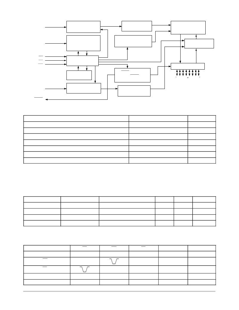
Figure 1. Block Diagram
Table 1. ABSOLUTE MAXIMUM RATINGS
Parameters
Temperature Under Bias
Storage Temperature
Voltage on Any Pin with Respect to Ground (Note 1)
V CC with Respect to Ground
Package Power Dissipation Capability (T A = 25 ° C)
Lead Soldering Temperature (10 secs)
Output Short Circuit Current (Note 2)
Ratings
–55 to +125
–65 to +150
–2.0 V to +V CC + 2.0 V
? 2.0 to +7.0
1.0
300
100
Units
° C
° C
V
V
W
° C
mA
Stresses exceeding Maximum Ratings may damage the device. Maximum Ratings are stress ratings only. Functional operation above the
Recommended Operating Conditions is not implied. Extended exposure to stresses above the Recommended Operating Conditions may affect
device reliability.
1. The minimum DC input voltage is ? 0.5 V. During transitions, inputs may undershoot to ? 2.0 V for periods of less than 20 ns. Maximum DC
voltage on output pins is V CC + 0.5 V, which may overshoot to V CC + 2.0 V for periods of less than 20 ns.
2. Output shorted for no more than one second. No more than one output shorted at a time.
Table 2. RELIABILITY CHARACTERISTICS (Note 3)
Symbol
N END
T DR
V ZAP
I LTH (Note 4)
Parameter
Endurance
Data Retention
ESD Susceptibility
Latch ? Up
Test Method
MIL ? STD ? 883, Test Method 1033
MIL ? STD ? 883, Test Method 1008
MIL ? STD ? 883, Test Method 3015
JEDEC Standard 17
Min
10 5
100
2,000
100
Max
Units
Cycles/Byte
Years
V
mA
3. These parameters are tested initially and after a design or process change that affects the parameters.
4. Latch ? up protection is provided for stresses up to 100 mA on address and data pins from ? 1 V to V CC + 1 V.
Table 3. MODE SELECTION
Read
Mode
CE
L
WE
H
OE
L
I/O
D OUT
Power
ACTIVE
Byte Write (WE Controlled)
Byte Write (CE Controlled)
L
L
H
H
D IN
D IN
ACTIVE
ACTIVE
Standby and Write Inhibit
Read and Write Inhibit
H
X
X
H
X
H
High ? Z
High ? Z
STANDBY
ACTIVE
http://onsemi.com
3
发布紧急采购,3分钟左右您将得到回复。
相关PDF资料
CAT310W-T1
IC LED DVR 10CH AUTO 20SOIC
CAT32TDI-T3
IC LED DRVR WHITE BCKLGT TSOT-6
CAT3604VHV4-GT2
IC LED DVR WHT CLR BACKLT 16TQFN
CAT3606HV4-T2
IC LED DRVR WHITE BCKLGT 16-TQFN
CAT3614HV2-T2
IC LED DRVR WHITE BCKLGT 12-TDFN
CAT3616HV4-GT2
IC LED DRVR WHITE BCKLGT 16-TQFN
CAT3636HV3-GT2
IC LED DVR 6CH QUAD MODE 16TQFN
CAT3643HV2-T2
IC LED DRVR WHITE BCKLGT 12-TDFN
相关代理商/技术参数
CAT28LV65WI-25
制造商:Catalyst Semiconductor 功能描述:
CAT28LV65WI-25T
功能描述:电可擦除可编程只读存储器 64K-Bit CMOS PARA 电可擦除可编程只读存储器 RoHS:否 制造商:Atmel 存储容量:2 Kbit 组织:256 B x 8 数据保留:100 yr 最大时钟频率:1000 KHz 最大工作电流:6 uA 工作电源电压:1.7 V to 5.5 V 最大工作温度:+ 85 C 安装风格:SMD/SMT 封装 / 箱体:SOIC-8
CAT28LV65XI-15
制造商:Rochester Electronics LLC 功能描述: 制造商:Catalyst Semiconductor 功能描述:
CAT30/41316L
制造商:MISCELLANEOUS 功能描述:
CAT-3000-01
制造商:Samtec Inc 功能描述:CAT - Bulk
CAT-3000-02
制造商:Samtec Inc 功能描述:CAT - Bulk
CAT310
制造商:ONSEMI 制造商全称:ON Semiconductor 功能描述:10 Channel Automotive LED Display Driver
CAT310_07
制造商:CATALYST 制造商全称:Catalyst Semiconductor 功能描述:10 Channel Automotive LED Display Driver
